THT-assembly
THT assembly of printed circuit boards
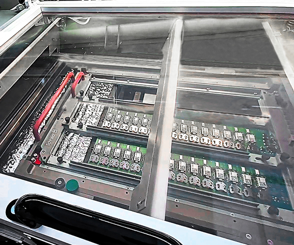
In THT assembly (THT=Through Hole Technology), wired components are placed in contact holes of printed circuit boards and soldered. THT assembly has been an important part of our service portfolio for more than 25 years. Our high-end machinery uses both wave and selective soldering processes. Customers from a wide range of industries benefit from our expertise.
Flexibility
Almost all printed circuit board and component shapes can be processed with our systems. Production is individually adapted to the respective assembly to be processed. Our state-of-the-art equipment enables us to process even the most complex components and assemblies.
Our resources allow us to flexibly and effortlessly implement customer change requests.
We manufacture medium and large series as well as smaller batches and prototypes.
Quality
By using the latest technology as well as high-quality materials, we offer our customers the highest product quality.
The soldering processes adapt flexibly to the requirements of the respective assembly. This guarantees gentle processing and minimizes the susceptibility to defects, which is also demonstrated by the following examples:
Before the soldering process, assemblies are gently heated to the ideal temperature. The setting of the optimum temperature in each case is automated. This results in homogeneous heating of the assemblies that is gentle on the components.
The innovative spray fluxer system ensures precise and reproducible flux application, which uniformly reduces the surface tension of the liquid solder. This results in consistently high solder quality.
The closed tunnel system with stable nitrogen atmosphere guarantees precise, optimum soldering results.
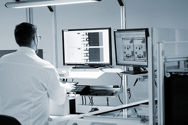
All relevant parameters are continuously monitored and documented, enabling both safe process performance and continuous optimization.
Efficiency
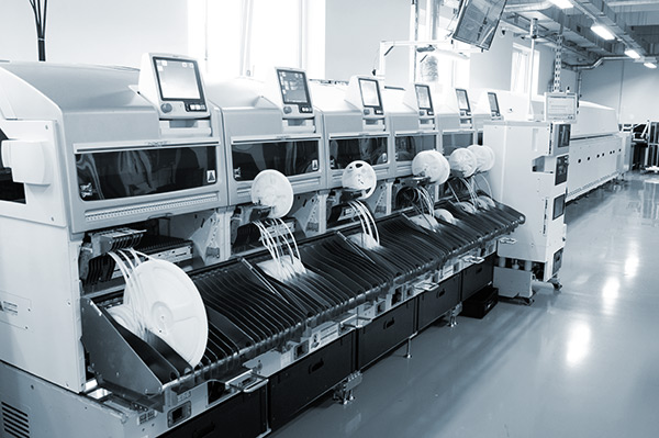
The idea of efficiency runs through our entire production. Our high-tech wave soldering area has an automated transport system that connects all components of the production line, thus guaranteeing an optimal production flow.
Several orders can be processed simultaneously, resulting in flexible and time-efficient work.
Sustainability
We are particularly concerned about the responsible use of resources. When purchasing new machines, we make sure that they operate energy-efficiently and that no resources are wasted. A perfect example of this is our new wave soldering system. Above all, the innovative fluxer system and the nitrogen tunnel stand out for their reduced consumption and resource-saving operation.
Numbers & Facts
| PCB format: | |
| PCB lenght: | 70 mm bis 450 mm |
| PCB Width: | 50 mm bis 380 mm |
| More formats on request | |
| components: | All components available on the market can be processed, z. B. 0205, 0402, 0603, 0805, 1020, 1206, 1210, 1806, 1812, 2010, 2512. Special components on request. |
| Max. Printed circuit board assemblies top: | 77 mm |
| Max. Printed circuit board assemblies below: | 30 mm |
| Lot sizes: | 1 – 50,000, also bigger lots are possible on request |
Numbers & Facts
LP length: 70 mm to 450 mm
LP width: 50 mm to 380 mm
Designs:
All components available on the market can be processed,
z. B. 0205, 0402, 0603, 0805, 1020, 1206, 1210, 1806, 1812, 2010, 2512.
Special components on request.
Max. PCB build-up top:
77 mm
Max. Printed circuit board superstructure bottom:
30 mm
Lot sizes:
1 – 50,000, larger lots are also available upon request.

Advantages at a glance
- Precision and speed with modern machinery and experienced employees.
- Flexibility for additions and order changes at short notice.
- Short and reliable delivery times through internal interface optimization and control processes.
- Material purchasing from proven suppliers on request.
- ISO 9001-certified quality management.
- Personal consulting by competent employees.
SMD assembly
In addition to the THT process, we assemble printed circuit boards using the SMD process.
Quality assurance
Quality monitoring measures include 3D solder paste inspection and Automatic Optical Inspection (AOI).
Request an offer now
Please contact us at the e-mail address vertrieb@baudisch.de and we will get back to you as soon as possible to work out your suitable offer.

Baudisch Electronic GmbH
Im Gewerbegebiet 19
73116 Wäschenbeuren
Newsletter subscription
Baudisch Electronic GmbH
Im Gewerbegebiet 19
73116 Wäschenbeuren
Newsletter subscription


