How the solder paste gets onto the circuit board
The application of solder paste is an important process step in SMT production. The solder paste is used to apply the components to the PCB and create an electrical connection between the two components. Another function is to prevent oxidation at the connections in the reflow oven.
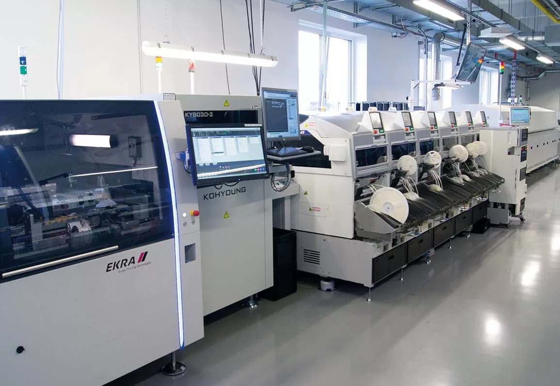
The solder paste can be applied using various methods. In SMT production at Baudisch Electronic, fully automatic screen printing technology is used, which enables particularly precise application in the shortest possible time. In this process, the solder paste is applied to the PCB using a specially manufactured stencil.
Both in the development phase and during SMT production, various criteria regarding the solder paste must be observed in order to ensure optimum quality of the assemblies.
Creating solder paste data
Before PCB assembly begins, data for the solder paste application is created. This contains all relevant information on the volume and placement of the solder deposits, the composition of the solder paste and the creation of the solder stencil. They are either provided by the customer or produced by our work preparation department on the basis of the PCB data.
The following criteria are defined in the solder paste data:
Soldering template
All details for creating the soldering stencil are defined. Among other things, the correct ratio between the size of the stencil opening and the stencil height must be observed. If the opening is too small for the height of the stencil, there is a risk that the solder paste will not be pressed completely through the stencil opening onto the PCB.
Shape, placement and height of the lot deposit
The volume of the solder deposit must be calculated precisely. Too much solder paste leads to overflow, too little can result in reduced adhesion and conductivity between the component and the PCB.
Properties of the solder paste
The type of paste is an important criterion for a clean solder paste application and is determined individually. For small components, for example, a special solder paste with a fine grain size is used, which can be easily spread into smaller stencil openings. The standard at Baudisch Electronic is a type 4 paste
Creation of the soldering stencil
The soldering stencil is specially manufactured for an assembly by our long-standing suppliers. The openings of the stencil correspond to the placement, volume and area of the solder deposit to be applied. The stencil is usually made of stainless steel and has a thickness of 80 µm to 120 µm. Stencils used in our production are prepared for a quick clamping system, which significantly speeds up the set-up time of our SMD production.
Processing the solder paste in the SMD production process

After a PCB has been provided with an individual data matrix code for complete traceability, the solder paste is applied fully automatically. To do this, the stencil is placed on the PCB. The solder paste is drawn over the stencil with a squeegee and pressed into the stencil openings.
The solder deposit is then checked in the 3D SPI (SPI = Solder Paste Inspection) for quality-critical parameters such as volume, offset and height. If a deviation from the target value is detected, the affected PCB is ejected. We immediately check whether there is a systematic error or whether it is a single deviation. If necessary, settings are adjusted and checked in the further course of production before series production continues. In this way, we ensure that the entire batch receives an optimum application of solder paste.
In the subsequent production process, the circuit board is fitted with components using Fuji NXT III placement machines. These are placed precisely onto the applied solder paste.
In the reflow oven, the solder paste is heated in a targeted manner so that the solder it contains melts. The soldering profile is individually adapted to the PCB design, the solder paste and the components used. The component and PCB are then firmly bonded together.
